Imagine packing tens of billions of transistors onto a piece of silicon no bigger than your fingernail. At this microscopic scale, absolutely zero margin for error exists in any step of the process. This is exactly where Metrology and Inspection step in. Acting as the "eyes" and the "quality inspectors" of chip manufacturing, these two core processes ultimately dictate a semiconductor's yield and performance.
I. First Things First: What is the difference between Metrology and Inspection?
Here is the core difference in a nutshell:
· Metrology (Measuring "Is it precise?"):
This involves measuring physical parameters like dimensions, film thickness, and overlay accuracy to ensure the chip perfectly matches its design blueprints.
· Inspection (Checking "Is it defective?"):
This is all about hunting for physical damage—such as stray particles, scratches, pattern defects, or contamination—to pinpoint the root causes of failure.
Without these critical quality control steps, mass-producing advanced node chips would be physically impossible, and manufacturing yields would plummet straight to zero.

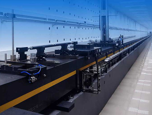
II. Metrology: The "Precision Calipers" of the Chip World
Metrology is responsible for accurately quantifying key parameters, ensuring that every single layer of the manufacturing process is executed flawlessly down to the nanometer.
1. Critical Dimension (CD) Metrology
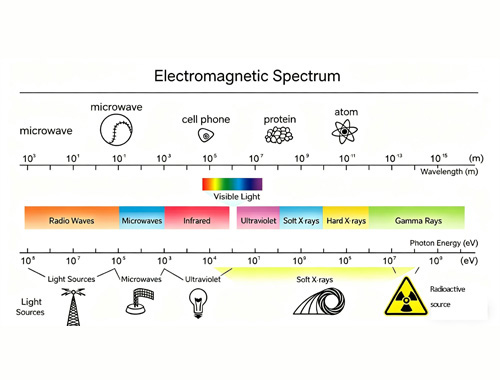
· CD-SEM (Critical Dimension Scanning Electron Microscope): Uses electron beams to measure nanoscale line widths and line-edge roughness.
· OCD (Optical Critical Dimension): A rapid, non-destructive optical scattering method that works perfectly hand-in-hand with CD-SEM.
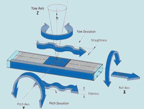
2. Overlay (OVL) Accuracy
When stacking multiple layers of circuitry, perfect alignment is non-negotiable. If the overlay error exceeds strict tolerances, the entire chip is immediately scrapped.
3. Film Thickness (THK)
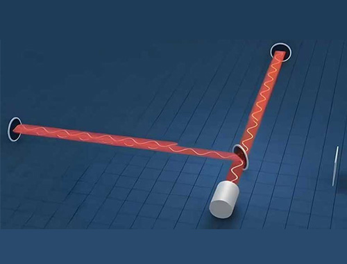
· Ellipsometry: The workhorse for measuring film thickness, boasting atomic-level precision.
· Spectral Reflectometry: Provides high-speed, inline monitoring perfectly paced for mass production rhythms.
4. Other Crucial Metrology Techniques
· Stress / Warpage Metrology: Prevents the silicon wafer from deforming or fracturing during processing.
· TSV (Through-Silicon Via) Metrology: Ensures the reliability of advanced 3D packaging technologies.
· Virtual Metrology: Utilizes AI to predict physical parameters without touching the wafer, maintaining high production capacity.

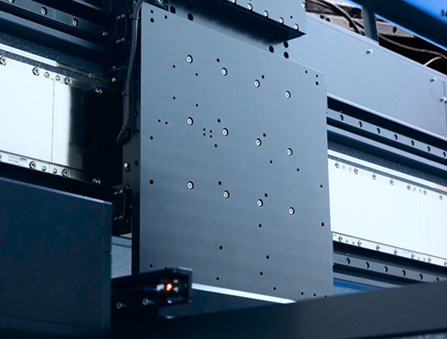
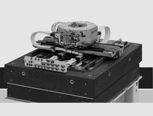
III. Inspection: The "Defect Hunter"
Inspection takes on the role of discovering, locating, and analyzing defects, acting as a vital checkpoint to filter out bad chips before they reach mass production.
1. Optical Inspection
As the most mature and widely used solution on the production line, it features high speeds and broad coverage, making it a standard piece of equipment. It includes:
· Brightfield / Darkfield Inspection
· Full-wafer surface defect scanning and particle detection.
2. E-Beam Inspection
When optical tools simply cannot "see" the ultra-tiny defects found in advanced manufacturing nodes, high-resolution electron beams take over to accurately identify these microscopic flaws.
3. Cutting-Edge High-Precision Inspection
· TSOM (Through-Focus Scanning Optical Microscopy): A rapid, non-destructive method for capturing nanoscale dimensions.
· AFM (Atomic Force Microscopy): Delivers ultra-high precision surface topography analysis.
· AI Defect Inspection: Leverages deep learning to automatically identify defects, vastly outperforming human inspection in efficiency.

IV. The Key to Mass Production: Balancing Precision and Efficiency
Inspecting every single chip would severely bog down production capacity and skyrocket costs. To counter this, modern production lines employ optimized strategies:
· Smart Sampling: Testing less but testing smarter, ensuring all critical bottleneck stations are covered.
· Statistical Process Control (SPC): Monitoring equipment stability in real-time.
· AI Virtual Metrology: Achieving full coverage with zero physical contact to drastically boost efficiency.
The Ultimate Goal: To achieve the highest possible yield at the lowest cost, all at the fastest production rhythm.

V. Conclusion: The Critical Chokepoint of Semiconductors
The more advanced the manufacturing process, the more vital Metrology and Inspection become. While these processes do not physically "build" the chips, they absolutely dictate whether a chip can be manufactured at all—and whether it will function properly.
As the industry saying goes:
Semiconductor manufacturing is established by the process, but won by metrology and inspection.